4-layer semiconductor packaging substrate
slp-pcbAvailability: In Stock
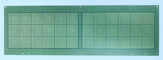
Product Description
This is a chip-scale package (CSP) substrate for IC substrates that is compatible with the wire bonding process. Its core lies in the connection between the chip and the substrate bonding fingers via wire bonding using gold wires/aluminum wires or other conductive wires. The package area is close to the chip size (typically, the chip area is ≥ 80% of the package area), and it is equipped with BGA solder balls on the back for interconnection with PCBs.
Specifications
- ●Layer Count:4L
- ●Material:HL832NXA
- ●Board Thickness:0.27mm
- ●Min.Trace/Space:2/2mil
- ●Surface Finsh: ENEPIG
- ●Copper paste plugging process
- ●Strict SM flatness control ≤5μm